Abis Circuits Co., Ltd.
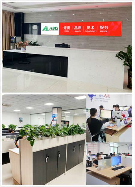
ABIS Circuits Co. Ltd, established in 2006, Located in Shenzhen,
our company has about 1100 workers and two PCB workshops with about
7.0000 square meters.
Our products are mostly used in the field of Industrial Control,
Telecommunication, Automotive products, Medical, Consumer, Security
and others.
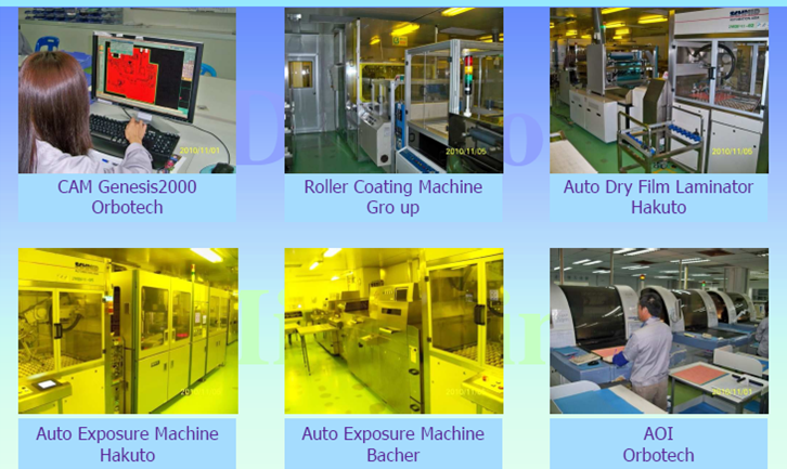
Our perfect management, advanced equipment, and professional staffs
are the keys for us to fight to win more market shares with other
competitors. Customer satisfaction and support are what we have
been strived for.
Now we have passed ISO9001, ISO14001, UL, etc., With constant hard
work of our staff and ongoing support from customers both home and
abroad, we can provide up to 20 layers, Blind and buried Board,
high-precision(Rogers), High TG, Aluminum base and flexible boards
to our customer with fast turn and high-quality level.