Professional Multilayer Printed Circuit Board HASL Electronic FR4
PCB Board
Product details
1. Single, Double side & Multi-layer PCB.
2. Buried/Blind Vias, Via in Pad, Counter Sink Hole, Screw
Hole(Counterbore), Press-fit, Half Hole.
3. HASL lead-free, Immersion Gold/ Silver/Tin, OSP, Gold
plating/finger, Peelable mask,
4. Printed Circuit Boards adhere to IPC Class 2 & 3 international
PCB standard.
5. Quantities range from prototype to medium&big batch
production.
6.100% E-Test.
Technical & Capability
| Item | Production Capacity |
| Layer Counts | 1-20 layers |
| Material | FR-4(High TG),Aluminum Base,Cu base,CEM1,CEM3,Polyimide,Halogen
free,Rogers,TEFLON etc. |
| Board thickness | 0.20mm-8.00mm |
| Maximum Size | 600mmX1200mm |
| Board Outline Tolerance | +0.10mm |
| Thickness Tolerance(t≥0.8mm) | ±8% |
| Thickness Tolerance(t<0.8mm) | ±10% |
| Insulation Layer Thickness | 0.075mm--5.00mm |
| Minimum Line | 0.075mm |
| Minimum Space | 0.075mm |
| Out Layer Copper Thickness | 18um--350um |
| Inner Layer Copper Thickness | 17um--175um |
| Drilling Hole(Mechanical) | 0.15mm--6.35mm |
| Finish Hole(Mechanical) | 0.10mm-6.30mm |
| Diameter Tolerance(Mechanical) | 0.05mm |
| Registration(Mechanical) | 0.075mm |
| Aspect Ratio | 16:1 |
| Solder Mask Type | LPI |
| SMT Mini.Solder Mask Width | 0.075mm |
| Mini. Solder Mask Clearance | 0.05mm |
| Plug Hole Diameter | 0.25mm--0.60mm |
| Impedance control Tolerance | ±10% |
| Surface finish/treatment | HASL-LF,ENIG,Hard gold plating,Immersion Tin/Silver,Flash Gold,
OSP, Gold Finger,Peelable mask etc |
Lead Time
| Category | Q/T Lead time | Standard Lead Time | Mass Production |
|
| 2 Layers | 24hrs | 3-4 working days | 8-15 working days |
|
| 4 Layers | 48hrs | 3-5 working days | 10-15 working days |
|
| 6 Layers | 72hrs | 3-6 working days | 10-15 working days |
|
| 8 Layers | 96hrs | 3-7 working days | 14-18 working days |
|
| 10 Layers | 120hrs | 3-8 working days | 14-18 working days |
|
| 12 Layers | 120hrs | 3-9 working days | 20-26 working days |
|
| 14 Layers | 144hrs | 3-10 working days | 20-26 working days |
|
| 16-20 Layers | Depends on the specific requirements |
|
| 20+ Layers | Depends on the specific requirements |
Multilayer PCB Production Range
| Number of layers | 4 – 22 layers standard, 30 layers advanced |
| Technology highlights | Multilayer boards with a higher connection pad density than
standard boards, with finer lines/spaces, smaller via holes and
capture pads allowing microvias to only penetrate select layers and
also be placed in surface pads. |
| HDI builds | 1+N+1, 2+N+2, 3+N+3,4+N+4, any layer in R&D |
| Materials | FR4 standard, FR4 high performance, Halogen free FR4, Rogers |
| Copper weights (finished) | 18μm – 70μm |
| Minimum track and gap | 0.075mm / 0.075mm |
| PCB thickness | 0.40mm – 3.20mm |
| Maxmimum dimensions | 610mm x 450mm; dependant upon laser drilling machine |
| Surface finishes available | OSP, ENIG, Immersion tin, Immersion silver, Electrolytic gold, Gold
fingers |
| Minimum mechanical drill | 0.15mm |
| Minimum laser drill | 0.10mm standard, 0.075mm advanced |
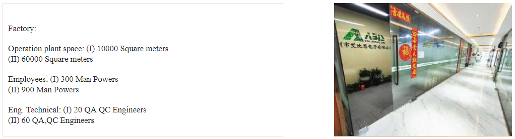
Company Profile
Abis Circuits Co., Ltd, a professional PCB manufacturer which was
established on Oct, 2006. Focus on double side, Multilayer and HDI
pcb mass production.
We have two factories together. The factory in Shenzhen is
specialized in small and middle volume orders. Another in Jiangxi
province is for big volume and HDI.
Our Mission
PCBs for demanding customers, on time with zero defects, produced
sustainably at the lowest total cost. Manufacturing many different
types of PCBs in smaller series (High-mix, Low-volume) involves
constantly adjusting, adapting and problem solving.
Pre-Sale and After-Sale Service
1 Hour quotation
2 hours complaint feedback
7*24 hour technical support
7*24 order service
7*24 hour delivery
7*24 production run
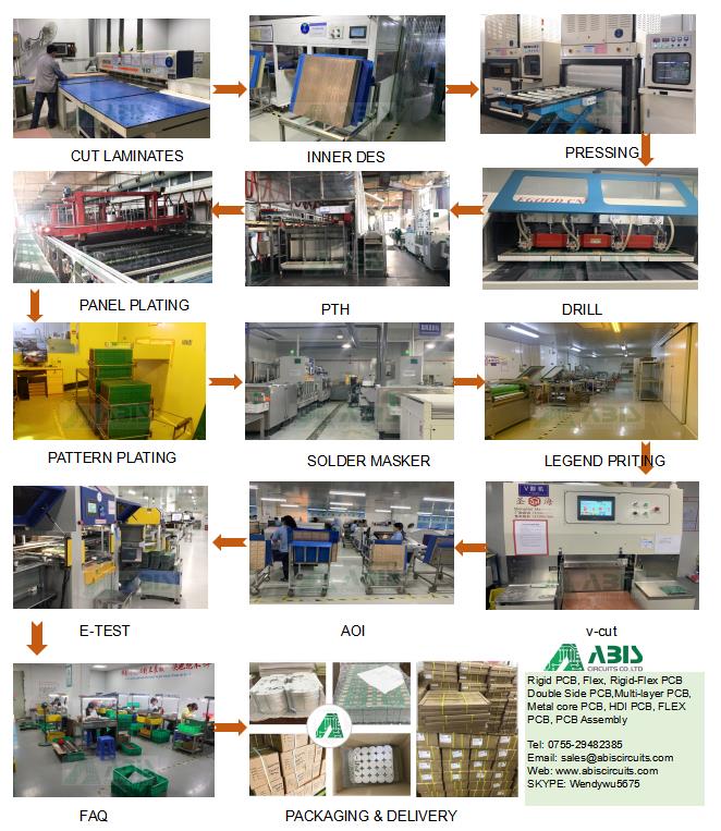
PCB Process
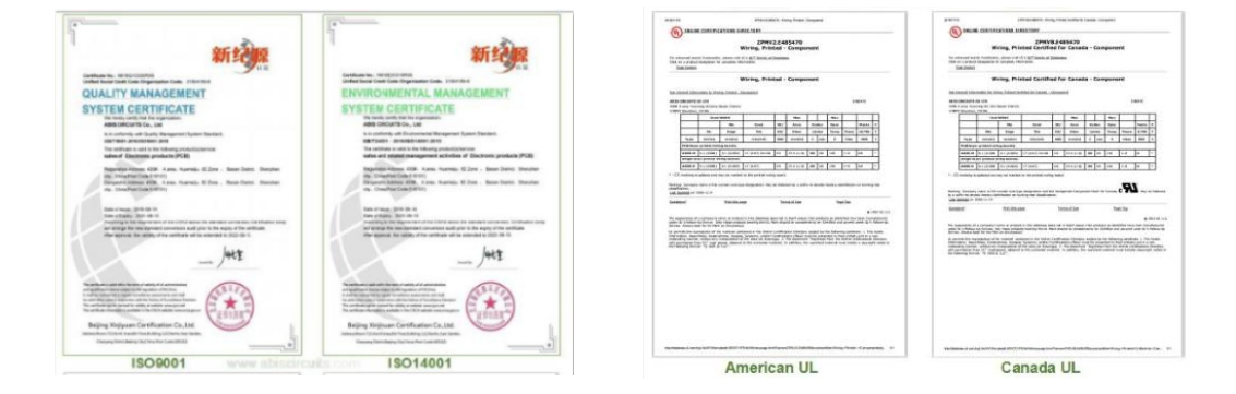
Certificate
Q1:Are you a factory or trade company?
A: Abis is a PCB/FPC/PCBA manufacturer/factory. We pecialize in
PCB/PCBA Board for 12 years.
Q2:Is my PCB file safe if I send it to you for manufacturing?
A: We respect customer's design authority and will never
manufacture PCB for someone else without your permission. NDA is
acceptable.
Q3:What is your testing policy and how you control the quality?
A: For sample, usually tested by flying probe; for PCB Volume over
3 square meters, usually tested by fixture, this will be more
faster. Due to there's many steps to PCB production, we usually do
inspection after every step.
Q4: What's your shipping way ?
A: 1. We have our own forwarder to ship goods by DHL, UPS, FEDEX,
TNT,EMS.
2. If you have your own forwarder, we can cooperate with them.
Q5: What is your certificate?
A: ISO9001:2015, ISO14001: 2015, UL, SGS,RoHS report.
Q6: Why choose us?
A: With ABIS, customers significantly and effectively reduce their
global procurement costs. Behind each service provided by ABIS, is
hidden a cost saving for customers.
. We have two shop together, one is for prototype, quick turn,
small volume making. The other is for mass production also for HDI
board, with highly skilled professional employees, for high quality
products with competitive price and on-time delivery.
. We provide very professional sales, technical and logistic
supports, on a world-wide basis.hours complaint feedback.
Please keep us informed for any interest!
ABIS cares every your order even 1 piece!