Prototype PCB ISO14001 35um Double Layer PCB Circuit Board 1.6mm
Thickness board
Company Abstract
Abis Circuits Co. Ltd, established in 2006, Located in Shenzhen, our company has about
1100 workers and two PCB workshops with about 50000 square meters.
Our products are mostly used in the field of Industrial Control,
Telecommunication, Automotive products, Medical, Consumer,
Security, and others.
Our perfect management, advanced equipment, and professional staffs
are the keys for us to fight to win more market shares with other
competitors. Customer satisfaction and support are what we have
been strived for.
Factory Overview
| Shenzhen | Jiangxi |
| Area | 10,000 Square meters | 60000 Square meters |
| Employees | 300 | 900 |
| Quality | 20 | 60 |
Administration | 5 | 10 |
| Engnieering | 20 | 90 |
Over Sales | 10 | 20 |
| Process Capability | |
|
| Material Type: FR4/Aluminum/Ceramic/CEM-1/Copper/polytef | Cooper thickness: 0.5-12OZ |
|
| Board Thickness: 0.25-6.0mm | Min hole size: 0.2mm( finished hole size) |
|
|
| Min Line Width/spacing:0.08mm | Drilling accuracy:+/-0.05 |
|
| Max working size:520*620mm(21.25x24.5inch) | Min Inner layer thickness:0.1mm |
|
| Min thickness Board for HAL surface finished:0.4mm | Certificate: Rohs, Iso9001, UL(in certification) |
|
|
| Min thickness 4 layer: 0.4mm | Min thickness 6 layer:0.6mm |
| Min/Max layer count : 1/20 | Lamination evenness :+/-0.05mm |
| Min SMD Pitch : 0.125mm | Min Dam Between Fine Pitch: >0.1mm |
| Layer to Layer registration:<0.1mm | Impedance control:+/-5% |
| Differential impedance:+/-10% | Board bow/twist tolerance:<0.7% |
| Plating spect ratio: <8:1 | Plating COV: <10% |
| Surface Finished: LF-HASL ,Immersion Gold/Tin/Silver ./Plating
Gold/OSP, | PTH backlight : 9-9.5 level |
| Solder Mask:Green , Red, Blue,White, Black,Yellow. | Plating extensibility:>15% |
Lead Time
| Category | Q/T Lead time | Standard Lead Time | Mass Production |
|
| 2 Layers | 24hrs | 3-4 working days | 8-15 working days |
|
| 4 Layers | 48hrs | 3-5 working days | 10-15 working days |
|
| 6 Layers | 72hrs | 3-6 working days | 10-15 working days |
|
| 8 Layers | 96hrs | 3-7 working days | 14-18 working days |
|
| 10 Layers | 120hrs | 3-8 working days | 14-18 working days |
|
| 12 Layers | 120hrs | 3-9 working days | 20-26 working days |
|
| 14 Layers | 144hrs | 3-10 working days | 20-26 working days |
|
| 16-20 Layers | Depends on the specific requirements |
|
| 20+ Layers | Depends on the specific requirements |
Packaging & Delivery
ABIS CIRCUITS Company is not only trying to give customers a good
product, but also pay attention to offering a complete and safe
package. Also, we prepare some personalized services for all the
orders.
-Common packaging:
- PCB: Sealed bag, Anti-static bags, Suitable carton.
- PCBA: Antistatic foam bags, Anti-static bags, Suitable carton.
- Customized Packaging: The carton outside will be printed the name
of the customer address, mark, the customer needs to specify the
destination and other information.
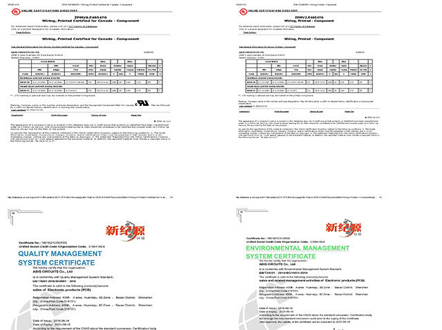
Certifications
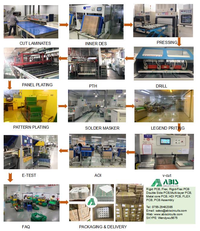
PCB Manufacturing Process
- The process starts with designing Layout of the PCB using any PCB
designing software / CAD Tool (Proteus, Eagle, Or CAD).
- All rest of the steps are of Manufacturing Process of a Rigid
Printed Circuit Board is same as Single Sided PCB or Double Sided
PCB or Multi-layer PCB.
Abis customer

FAQ
Q1: How can I get a quotation?
. Please send gerber file with format: .PCB / .P-CAD / .DXP / .Gerber
Q2: Can you manufacture my PCBs from a picture file?
. Could you please provide a sample?
Q3: Do you have PCB in stock?
. Most of our PCB board are customized, which according to Gerber file.
. ABIS has samples in stock that could be sent to you for quality
checking always.
Q4: What board manufacturer do you use for FR4?
. Main Suppliers(FR4): Kingboard (Hong Kong), NanYa (Taiwan), and
Shengyi (China).
Q5: Will my PCB files be checked?
. Checked within 12 hours. Once Engineer's question and working
file be approved, production will start.
Q6: What do you require in order to produce an assembly quotation?
. Bill of materials (BOM) detailing:
a), manufacturers parts numbers,
b), components suppliers' parts number (e.g. Digi-key, Mouser, RS )
c), PCBA sample photos if possible.
d), Quantity
plexity.


