0.5MM FR4 HASL 4 Layer Prototype PCB Board X RAY Inspection Pcb
Making Service Pwb Assembly
PCB Production Range
| Number of layers | 4 – 22 layers standard, 30 layers advanced |
| Technology highlights | Multilayer boards with a higher connection pad density than
standard boards, with finer lines/spaces, smaller via holes and
capture pads allowing microvias to only penetrate select layers and
also be placed in surface pads. |
| HDI builds | 1+N+1, 2+N+2, 3+N+3,4+N+4, any layer in R&D |
| Materials | FR4 standard, FR4 high performance, Halogen free FR4, Rogers |
| Copper weights (finished) | 18μm – 70μm |
| Minimum track and gap | 0.075mm / 0.075mm |
| PCB thickness | 0.40mm – 3.20mm |
| Maxmimum dimensions | 610mm x 450mm; dependant upon laser drilling machine |
| Surface finishes available | OSP, ENIG, Immersion tin, Immersion silver, Electrolytic gold, Gold
fingers |
| Minimum mechanical drill | 0.15mm |
| Minimum laser drill | 0.10mm standard, 0.075mm advanced |
Testing
E-testing | 100% |
QFP Pitch | 16mil (0.40mm) |
BGA Pitch | 16mil (0.40mm) |
Connector Pitch | 16mil (0.40mm) |
AOI | All Multilayer |
Impedance Control | ± 10% |
Solderability Testing | As standard |
Ionic Contamination | On Request |
Our Lead Time
| Number of Layers | Quick Turn Lead Time |
| 2 | 24 Hours |
| 4 | 48 Hours |
| 6 | 72 Hours |
| 8 | 96 Hours |
| 10 | 120 Hours |
| 12 | 120 Hours |
| 14 | 144 Hours |
| 16 | Depend on Technical Specification |
| 18 | Depend on Technical Specification |
| 20 | Depend on Technical Specification |
Delivery Time
Air Freight Lead Time – 4 Days |
Sea Freight Lead Time – 30 Days |
All Far East lead times are subject to customs clearance |
Premium International shipments can be arranged by DHL, Fedex, UPS
or TNT at extra cost |
Product Application
1, Consumer Electronics: TV, DVD,Digital Caramer, air conditoner,
Refrigerator,set-top box etc;
2, Security monitor: Moible phone, PDA, GPS, caramer monitor etc;
3, Telecom Communication :wireless LAN card, XDSL router,Servers,
Optical Device,Hard Drive etc;
4, Industrial controls: Medical device ,UPS equipment, Control
device etc;
5, Vehicle Electronices: Car etc;
6, Military & Defense : Military Weapons etc;
Product We Produce
1. Rigid, Flex, Rigid-Flexible PCB.
2. Buried/Blind Vias, Via in Pad, Counter Sink Hole, Screw
Hole(Counterbore), Press-fit, Half Hole.
3. HASL lead-free, Immersion Gold/ Silver/Tin, OSP, Gold
plating/finger, Peelable mask,
4. Printed Circuit Boards adhere to IPC Class 2 & 3 international
PCB standard.
5. Quantities range from prototype to medium & big batch
production.
6. 100% E-test
Company Profile
Abis Circuits Co. Ltd, established in 2006, Located in Shenzhen,
our company has about 1100 workers and two PCB workshops with about
50000 square meters. Our products are mostly used in the field of
Industrial Control, Telecommunication, Automotive products,
Medical, Consumer, Security, and others.Now we have passed ISO9001,
ISO14001, UL, etc., With constant hard work of our staff and
ongoing support from customers both home and abroad, we can provide
up to 20 layers, Blind and buried Board, high-precision(Rogers),
High TG, Alu-base and flexible boards to our customer with fast
turn and high-quality level.
Our mission
PCBs for demanding customers, on time with zero defects, produced
sustainably at the lowest total cost. Manufacturing many different
types of PCBs in smaller series (High-mix, Low-volume) involves
constantly adjusting, adapting and problem solving. We know that the PCB is a critical key component for our customers.
And we know for sure that anything can happen during the complex
production process involved – and it often does. In our world,
taking full responsibility means a lot of things, including a
responsible and sustainable approach in everything we do –
socially, environmentally and ethically. When a problem occurs, we
try as hard as we can to understand the problem and find a
solution. Our mindset is that we own the problem and don’t leave
until we have cleared it up.
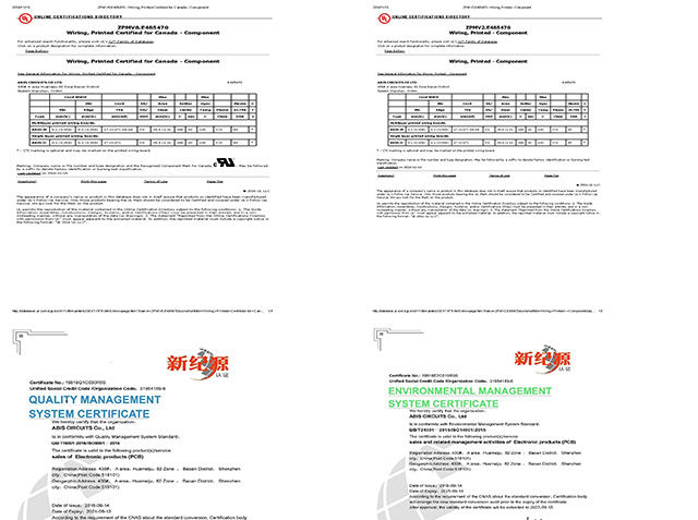
Certifications
WorkShop

Customer Visit

FAQ
1. How do ABIS ensure quality?
Our high quality standard is achieved with the following.
1.1 The process is strictly controlled under ISO 9001:2008
standards.
1.2 Extensive use of software in managing the production process
1.3 State-of-art testing equipments and tools. E.g. Flying
Probe,e-Testing, X-ray Inspection, AOI (Automated Optical
Inspector) .
1.4.Dedicated quality assurance team with failure case analysis
process
2. What kinds of boards can ABIS process?
Common FR4, high-TG and halogen-free boards, Rogers, Arlon, Telfon,
aluminum/copper-based boards, PI, etc.
3. What data are needed for PCB production?
PCB Gerber files with RS-274-X format.
4. What’s the typical process flow for multi-layer PCB?
Material cutting → Inner dry film → inner etching → Inner AOI →
Multi-bond→ Layer stack up Pressing → Drilling → PTH → Panel
Plating → Outer Dry Film → Pattern Plating → Outer etching → Outer
AOI → Solder Mask → Component Mark → Surface finish → Routing → E/T
→ Visual Inspection.
5. How many types of surface finish ABIS can do?
the leader has the full series of surface finish, such as: ENIG,
OSP, LF-HASL, gold plating (soft/hard), immersion silver, Tin,
silver plating, immersion tin plating, carbon ink and etc. .. OSP,
ENIG, OSP + ENIG commonly used on the HDI, we usually recommend
that you use a client or OSP OSP + ENIG if BGA PAD size less than
0.3 mm.
6. What are the main factors which will affect the price of PCB?
Material;
Surface finish;
Board thickness, Copper thickness;
Technology difficulty;
Different quality criteria;
PCB characteristics;
Payment terms;


